
The precision required to manipulate matter at the atomic level has historically been limited by the observational lag between synthesis and characterization, but recent breakthroughs are finally closing this gap. Modern laboratories are transitioning from static imaging to dynamic, in-situ monitoring where researchers witness molecular assembly as it happens in real-time. This evolution is driven by ultra-fast electron microscopy and advanced scanning probe systems that offer picometer resolution while maintaining environmental control. As industries demand more complex carbon nanotubes and quantum dots, the need for real-time feedback loops has never been more critical than it is today. These tools do not merely provide a clearer picture; they allow for a fundamental shift in how scientists approach chemical vapor deposition. By integrating machine learning algorithms directly into the sensor arrays, instruments now predict structural defects before they propagate. This capability transforms nanomaterial engineering from a trial-and-error process into a high-fidelity manufacturing discipline where every atom is accounted for.
High-Resolution Imaging: Bridging the Gap Between Observation and Manipulation
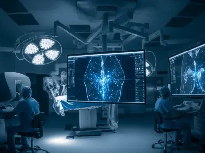
Modern transmission electron microscopes have evolved beyond simple imaging platforms to become comprehensive laboratories that allow for the simultaneous application of heat, pressure, and electrical stimuli. By utilizing direct electron detectors and aberration correction technologies, these instruments capture the movement of individual atoms during phase transitions or chemical reactions without damaging the sensitive specimens. This level of detail is essential for developing the next generation of solid-state batteries and high-efficiency catalysts, where the interface between different materials determines the overall performance. Furthermore, the development of liquid-cell microscopy has enabled the study of nanoparticles in their natural, fluid environments, providing insights into biological interactions and electrochemical processes. These advancements ensure that researchers no longer rely on post-mortem analysis of samples, but instead gain a comprehensive understanding of material behavior.
Parallel to the advancements in electron-based systems, scanning probe microscopy has seen a resurgence through the implementation of multi-frequency atomic force microscopy and high-speed scanning techniques. These instruments now achieve frame rates that allow for the visualization of surface diffusion and molecular self-assembly on timescales previously thought impossible for mechanical probes. By utilizing ultra-sharp tips and sophisticated feedback controllers, engineers can map the electronic and mechanical properties of a surface with sub-nanometer lateral resolution while simultaneously measuring local conductivity. This dual capability is particularly valuable in the semiconductor industry, where the transition to sub-three-nanometer nodes requires precise control over dopant distribution. The integration of spectroscopic capabilities allows for the identification of chemical species at the single-molecule level. Such precision provides a robust foundation for the bottom-up fabrication of molecular electronics.
Future Integration: Standardizing Data and Scaling Production
The marriage of robotic automation and high-throughput characterization has led to the rise of autonomous closed-loop synthesis platforms that significantly accelerate material discovery. These systems utilize sophisticated software to design experiments, execute synthesis protocols, and analyze the resulting data without human intervention, allowing for the exploration of vast chemical spaces in a fraction of the time. For instance, in the development of perovskite solar cells, automated dispensers and spin-coaters can test thousands of precursor combinations to optimize grain size and crystallinity for maximum efficiency. High-speed optical sensors and X-ray diffraction units integrated into the assembly line provide immediate quality control, feeding results back into the control algorithm to refine the next iteration. This shift toward data-driven engineering reduces the reliance on serendipitous discovery and instead focuses on systematic optimization through Bayesian statistics.
Addressing the remaining challenges in nanomaterial engineering necessitated a transition toward standardized data formats and open-source collaborative frameworks that facilitated the global exchange of experimental results. Researchers established rigorous protocols for instrument calibration and data metadata, ensuring that findings from one facility were directly comparable to those from another across the globe. This unified approach allowed for the creation of massive material property databases that served as the training grounds for the next generation of predictive models. Practical steps included the widespread adoption of cloud-based analysis tools and the implementation of blockchain for secure, transparent tracking of material provenance. Scientists focused on scaling these precision techniques from milligram-level laboratory outputs to ton-scale industrial manufacturing, ensuring that the benefits of nanotechnology reached the consumer market. This prioritized the integration of multi-modal sensing.