
The relentless pursuit of faster, more efficient computing has pushed traditional silicon-based electronics to their physical limits, prompting a shift toward photonic systems that utilize light rather than electrons. While fiber optics have already mastered long-distance data transmission, the challenge of processing that information at the chip level remains a significant hurdle due to the bulky nature of current optical components. Recent breakthroughs in nanotechnology have introduced a compelling solution involving chiral carbon nanotubes, which possess a unique structural “handedness” that allows them to interact with light in ways previously thought impossible. By isolating these specific structures and organizing them into highly ordered, macroscopic films, researchers have unlocked a massive light-conversion effect that could fundamentally alter the architecture of future processors. This development is not merely a marginal improvement but a significant leap in how light is manipulated at the nanoscale.
Breakthroughs in Light Conversion Efficiency
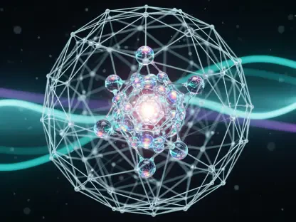
The core of this technological advancement lies in the phenomenon of second harmonic generation, where two photons of a specific frequency interact with a material to produce a single photon with twice the energy. In traditional materials, this process is often inefficient, requiring long interaction paths or high power levels to achieve meaningful results, which limits their use in compact circuitry. However, by utilizing crystalline films of single-chirality carbon nanotubes, scientists have observed conversion rates that are two to three orders of magnitude more efficient than those found in standard industrial materials. This “giant” optical response is driven by the one-dimensional nature of the nanotubes, which confines electrons and holes into coupled states known as excitons. These excitons amplify the nonlinear interaction between light and matter, allowing for a seamless transformation of invisible infrared signals into visible light with unprecedented precision and minimal energy loss.
Beyond the raw efficiency of frequency doubling, the scalability of these carbon nanotube films represents a major milestone in material science and optical engineering. Historically, the potential of carbon nanotubes was theoretical because raw batches contained a chaotic mix of right-handed and left-handed structures that effectively canceled out each other’s optical properties. The ability to isolate specific chiralities and then align them into centimeter-scale, wafer-like films has transformed these nanotubes from laboratory curiosities into viable industrial components. This alignment ensures that the chiral response is uniform across the entire surface, preventing the destructive interference that plagued earlier experiments. As a result, engineers now have access to a flexible, lightweight medium that can be integrated directly into existing semiconductor manufacturing processes, providing a pathway to hybrid systems that combine traditional logic with high-speed photonic processing.
Integration With Next-Generation Photonic Circuitry
The practical application of chiral nanotubes extends far beyond simple light conversion, as their unique physical properties allow for the creation of ultra-compact optical modulators and switches. In current light-based computing prototypes, the equipment required to change light frequency or phase often occupies significant space, making on-chip integration a logistical nightmare. Because carbon nanotubes are inherently one-dimensional and incredibly thin, they can be layered into multi-functional stacks without adding significant bulk or thermal load to the system. This allows designers to envision a new class of “all-optical” logic gates where light signals interact directly within the nanotube film to perform calculations. By removing the need for frequent optical-to-electrical conversions, these systems can operate at terahertz speeds while consuming a fraction of the power required by conventional high-performance computing clusters.
Furthermore, the mechanical flexibility of these nanotube films opens doors for advanced optoelectronics in unconventional form factors, such as wearable sensors and curved architectural interfaces. Unlike the brittle crystals typically used for nonlinear optics, these macroscopic nanotube wafers can be bent or integrated into flexible substrates without losing their high-performance light-conversion capabilities. This versatility is particularly relevant as the industry moves toward 2027 and 2028, where the demand for integrated photonics in telecommunications and artificial intelligence hardware is expected to skyrocket. By providing a material that is both highly efficient and physically resilient, researchers have solved one of the primary material science bottlenecks in the development of silicon photonics. This enables the creation of more robust and portable devices that maintain high-speed data integrity even under physical stress or varying environmental conditions.
Future Directions: Scaling and Implementation
To move this technology from successful laboratory validation into mass-market production, the next logical step involves refining the industrial synthesis of high-purity chiral films. While the Rice-led international team has proven that centimeter-scale films can be produced, the industry must now focus on developing automated sorting and deposition techniques that can handle larger wafer sizes consistent with modern fabrication facilities. Engineering teams should prioritize the development of standardized interfaces between these chiral films and traditional silicon-on-insulator platforms to ensure seamless data flow. This will likely involve optimizing the chemical vapor deposition processes to ensure that nanotube alignment remains perfect over larger surface areas. Success in this area will allow manufacturers to treat carbon nanotube layers as just another specialized coating in the complex stack of a modern microprocessor, simplifying the transition to light-based logic.
Moreover, the long-term viability of light-based computing will depend on how effectively these materials can be tuned for different wavelengths across the electromagnetic spectrum. Future research should explore the use of different nanotube diameters and chiralities to create a “toolkit” of films, each optimized for specific optical tasks such as signal amplification, frequency shifting, or polarization control. Stakeholders in the telecommunications and aerospace industries would benefit from investing in pilot programs that test these chiral films in high-radiation or high-temperature environments, where traditional electronics often fail. By aggressively pursuing these practical implementation strategies, the tech industry can transition away from the power-hungry constraints of copper and silicon. The focus shifted toward a future where light-driven processors provide the necessary bandwidth for the next decade of digital evolution, ensuring that computing power continues to grow without hitting a thermal ceiling.